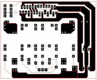
But it had a major constraint – 6 nos of jumper wires connecting the IC. I wanted to avoid that, so I redesigned the PCB. One very good thing I came to know about from DiyAudio was the use of n/c pins. So this was the All new third version. This came out to be most compact and straight layout. I made around 10 PCBs of this one.
This one is the latest. I tried to remove 2 more jumpers from V++ supply track and further thicken the power supply tracks. Mmm, still thinking to go for another version, little spacious this time. Troubleshooting become difficult in compact PCBs.


5 comments:
how do you have so much patience???
not patience, but i had little time to do this all. so slowly i kept on working...
Hi bro!!! I've been try you PCB already. It's working very well. Thank & Cheers
Could you please send me the pcb layout that can be used for toner transfer method...
Thank You.
wgoncharov1960@mail.ru
Post a Comment